9 Measures for Electrostatic Discharge (ESD)
9.2 ESD-proof Measures during Operations
9.3 ESD-proof Measures after Mounting
9.5 ESD Sensitivity Testing Models for Semiconductor Devices
9.1. General Precautions
1) Working Environment
A standard static electricity level, which ensures an ESD-safe working environment suitable for handling semiconductor devices, is generally regarded to be at 100 V or less. To ensure such environment, please be sure to avoid putting ESD-prone materials in your working area, and to humidify your working area during a dry time of year.。
2) Working Practices
Please be sure to avoid using insulators that are easily electrostatically charged (e.g., chemical fibers, plastics), and to use conductive or static-dissipative materials in your workstation. When handling ESD-sensitive semiconductor devices in particular, please wear antistatic working clothes and shoes. When storing such semiconductor devices, please be sure to take measures such as using antistatic or conductive containers. In addition to what is mentioned above, installing humidifiers or ionizers as needed is also an effective ESD-safe working practice.
3) Periodic Inspections
Please conduct periodic inspections to measure and check the following: the amounts of static charges on facilities/equipment and jigs/fixtures ; the resistance between antistatic mats and ground; the resistance on antistatic items (e.g., floors, wrist straps, shoes); the neutralization capabilities of ionizers, and so on. Please note that especially the neutralization capability of an ionizer will decrease unless its electrode needle tips are periodically cleaned or replaced, according to instruction manuals provided by the manufacturer.
9.2. ESD-proof Measures during Operations
1) Facilities and Equipment, Jigs and Fixtures
To prevent the buildup of static electricity, please be sure to ground the following: testing equipment and devices, conveyors, production facilities and equipment, workbenches, floor mats, tools, solder baths, soldering irons, and so on. Please also ground the shelves and utility carts used for storing and transferring products.
When soldering a semiconductor device to a PCB with a soldering iron, please use a semiconductor-dedicated soldering iron and ground its tip.
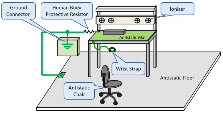
Example: ESD-safe Workstation

As for working surfaces, please put antistatic mats on a workbench top and a workstation floor, and then ground them respectively.
Example: ESD-safe Workbench and Floor

As for utility carts, please use the ones with conductive shelves and the conductive casters that can ground to antistatic floors.
Example: Utility Cart Grounded from Antistatic Casters to Antistatic Floor

2) Operators
Operators must wear ESD-safe clothing (e.g., antistatic working clothes and shoes) and connect the human body to the ground with a personal grounding device like a wrist strap.
An appropriate resistance of antistatic shoes is generally regarded to range from 100 kΩ to 100 MΩ. Contaminated shoe soles or floors will reduce static elimination effects. So please conduct periodic cleaning.
Example: Antistatic Working Clothes and Shoes

As for wrist straps, please be sure to use a corded wrist strap and ground it during operations. Cordless wrist straps are said to be unable to eliminate charged potentials completely and thus a voltage of approximately 200 V can be left on the human body. When grounding a wrist strap, please be sure to use a dedicated grounding jig, not an alligator clip or insulated (plastic-covered) alligator clip. Improper grounding, such as by clamping a bare copper wire with an alligator clip, may oxidize the surface of the bare copper wire over time, leading to insufficient discharge effects.
● Notes on Using Humidifier
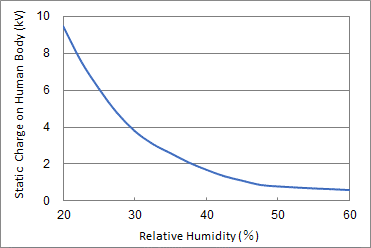
An environment with a humidity of 30% to 40% or less will cause a rapid and large increase in electrostatic charge generation. Therefore, keeping humidity at 45% or more is considered appropriate to ensure an ESD-safe working environment for handling semiconductor devices.
A typical electrostatic charge generation source that causes a substantial amount of the static charge built on the human body is a person with insulative shoes walking on a carpet. The graph below illustrates how humidity relates to the static charge built on the human body.
Reference: Static Charge vs. Humidity

When using a humidifier to maintain an appropriate humidity, please use purified water to prevent rust on terminals. When using tap water, please remove chlorine by boiling or by other means in order to reduce any causes of rust before use.
Most of semiconductor device packages use epoxy-based resins with high moisture-absorbing property. Therefore, the semiconductor devices stored at high humidity may cause deterioration in the characteristics and rust on the terminals. In particular, please note that the semiconductor devices packed in moisture-barrier materials are easily affected by humidity.
● Notes on Using Ionizer
Please use ionizers as needed in the following working environments: when charged potentials cannot be eliminated by grounding as an ESD-proof measure; when operations involve peeling; when operations generate friction. Before installing an ionizer, please consider its specifications (e.g., effective neutralization range) and determine how many ionizers to allocate in a working space to be installed. Here is the general guideline for periodic checks and maintenance to maintain the neutralization performance of the ionizer used.
[Periodic Check]
● Check neutralization capability
● Check ionic balance
[Periodic Maintenance]
● Clean electrode needles regularly
● Replace electrode needles regularly
For more details, please refer to the instruction manual provided and contact the manufacturer for any questions.
3) Operation Practices
To reduce ESD breakdowns of semiconductor devices, please be sure to minimize the handling frequency and handling time per semiconductor device.
9.3. ESD-proof Measures after Mounting
1) Storage
When storing or transferring the PCBs with semiconductor devices mounted on (i.e., PCB assemblies), please store them into antistatic containers. When storing the PCB assemblies, please be careful not to pile themselves or their populated components on top of each other and not to place them in contact with each other.
2) Handling
When handling the PCBs with semiconductor devices mounted on (i.e., PCB assemblies), please ground the operator’s human body with a personal grounding device like a wrist strap. When handling the PCB assemblies, please pay attention to electrostatic charge generation as well as the precautions for mounting semiconductor devices to PCBs. Before inserting into or removing from a connector, please be sure to turn off the power.
9.4. Human Body Protection
Human body grounding is one of the effective ESD-proof measures. However, when a grounded operator gets an electric shock, the operator’s human body will be exposed to dangers worse than normal conditions. To manage both ESD protection and human body protection successfully, please connect a resistor of approximately 1 MΩ in series between the operator’s human body and the ground. The larger the resistance, the less the antistatic effects of human body grounding. On the other hand, the smaller the resistance, the larger the current flows through and endanger the operator’s human body upon electric shock. In general, commercially available wrist straps have a built-in resistor of 1 MΩ or so.
9.5. ESD Sensitivity Testing Models for Semiconductor Devices
Actual static electricity applied to semiconductor devices differs in voltages and pulse widths among charged objects, materials, and sizes. Accordingly, using the ESD sensitivity testing models specified by international standards is the most commonly accepted method for quantitatively measuring the ESD withstand capabilities of semiconductor devices.
Here we introduce the overviews of the general standards.
1) Human Body Model (HBM)
This model is designed on the simulation that a discharge occurs from an electrically charged human body upon contact with a semiconductor device. A capacitor of 100 pF is charged by applying a voltage and is disconnected from the power supply when fully charged. Then, the energy stored in the capacitor discharges through a discharging resistor of 1.5 kΩ connected in series to the semiconductor device. The applied voltage at which the semiconductor device starts to deteriorate is determined as an electrostatic breakdown voltage. 。
2) Machine Model (MM)
This model is designed on the simulation that the energy charged in the capacitor of a device discharges to a semiconductor device. Please note that this model has been currently demoted to a reference standard, although called the “Japan model” as it was employed by the JEITA standards (the former EIAJ standards). A capacitor of 200 pF is charged by applying a voltage and is disconnected from the power supply when fully charged. Then, the energy stored in the capacitor discharges through a discharging resistor of 0 Ω to the semiconductor device. The applied voltage at which the semiconductor device starts to deteriorate is determined as an electrostatic breakdown voltage.
3) Charged Device Model (CDM)
This model is designed on the simulation as follows: A semiconductor device, which is electrostatically charged by the friction with a jig/fixture or the proximity of an electrically charged object, allows its internal components (e.g., a chip connected to the terminals) to be electrically charged. Then, the energy charged inside the semiconductor device discharges externally from the terminals. A voltage is applied between the semiconductor device’s terminals and package so that the internal components become electrically charged. After the power supply is disconnected, the internal charge discharges through a discharging resistor of 1 Ω from the terminals to the ground. The applied voltage at which the semiconductor device starts to deteriorate is determined as an electrostatic breakdown voltage.
4) Charged Package Model (CPM)
This model is designed on the simulation that the energy charged on a semiconductor device’s package, which is inductively charged by a high electrical field, discharges externally from the terminals. A high voltage is applied to the semiconductor device’s package to generate an inductive charge on it. The energy charged on the package then discharges through a discharging resistor of 0 Ω from the terminals to the ground. The applied voltage at which the semiconductor device starts to deteriorate is determined as an electrostatic breakdown voltage.
Questions or Comments?
Please feel free to contact us if you cannot find the desired product from the lineup.
